
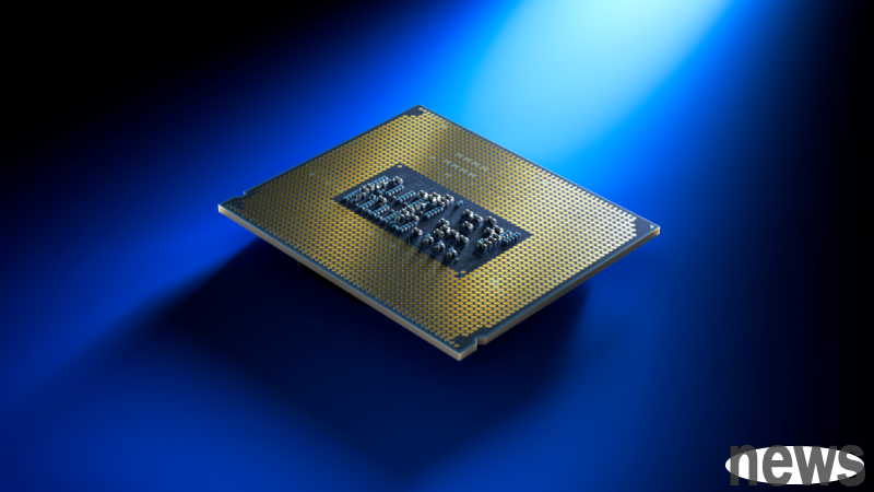
Intel explains advanced packaging applications of disaggregated heat sinks, targeting data center needs
In a paper titled "A New Disassembled Integrated Heatsink Assembly Method for Advanced Packaging," Intel engineers outlined the company's new method of manufacturing large and complex chip packages more efficiently and effectively, achieving better heat dissipation performance.
As shown in the article, this solution replaces a bulky single radiator with multiple modular parts that are simpler and easier to manufacture and assemble. The core of the design of "disaggregated heat sinks" like Intel's is to solve an increasingly serious problem, that is, the size of modern CPUs and GPUs is getting larger and larger, and traditional manufacturing methods are approaching their limits. Once the die package area exceeds approximately 7,000 square millimeters, conventional stamping dies cannot process the complex shapes required for stepped cavities and multi-die layouts. Even though digital control processing can do the job, it is slow, costly and difficult to scale.
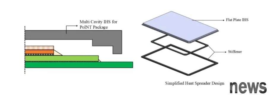
Intel’s new approach can cleverly avoid these problems by splitting the radiator into multiple smaller parts. Parts such as flat panels and reinforced structures can be produced using standard stamping techniques and then assembled like a jigsaw puzzle. This modular design not only simplifies the production process, but also improves efficiency.
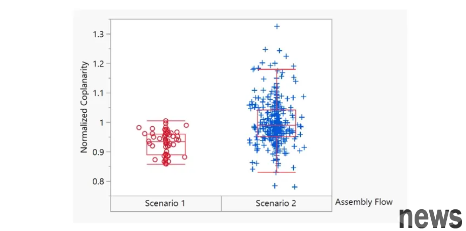
According to Intel's internal testing, this design can reduce the overall package warpage by approximately 30%, reduce the void ratio of the thermal interface material (TIM) by 25%, and improve coplanarity by approximately 7%. This means a flatter chip, better contact between components, and more efficient heat dissipation. These advantages will significantly improve long-term reliability and thermal efficiency for high-power chips manufactured with advanced packaging technologies such as Foveros or EMIB.
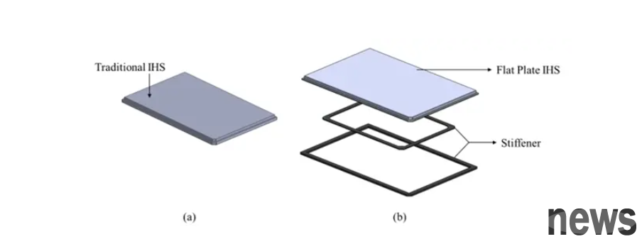
Exteriorly, this new architectural design replaces the traditional integrated heat sink (IHS) with a flat metal plate supported by structural reinforcements and an adhesive layer. These reinforcements maintain mechanical stability and create the cavities required for stacked or multi-die designs, resulting in heat sinks that perform as well as or better than traditional single-die designs, but at a much lower production cost.
Intel's paper focuses on how this approach fits perfectly with its "advanced packaging" approach. As the company moves deeper into 3D stacking and heterogeneous computing modules, packaging challenges become as important as shrinking transistor sizes. This new heat sink concept provides a way to build "very large" chip components that were previously considered too costly or impractical.
Researchers also hinted at the future application prospects of this technology. Intel plans to extend this approach to advanced thermal materials, such as highly thermally conductive metal composites and even water-cooled heat sink modules. Future data center products are expected to consume more than 600 watts of CPU and GPU power, so innovations like these are critical to controlling cooling.
Recommend News
-
Intel claims US government to invest in a stake in order to prevent the abandonm
-
Zhending SEMICON reveals PCB cross-semiconductors! Once again, we will work on r
-

Intel s privatization: Strategic solution or financial game?
-
Taiwan Electric 2 nanometer leak case investigation may cause shock in semicondu